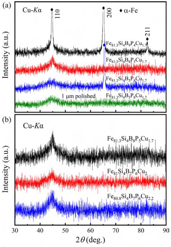
XRD patterns of the free surface of FeSiBPCu melt-spun alloy ribbons.
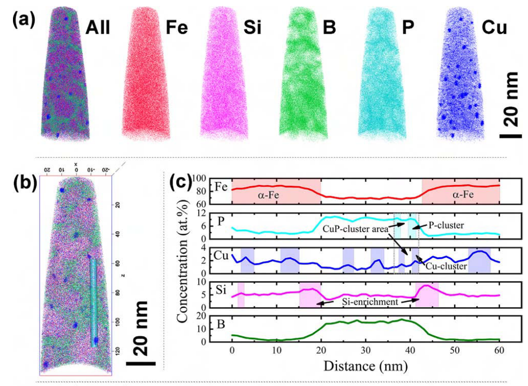
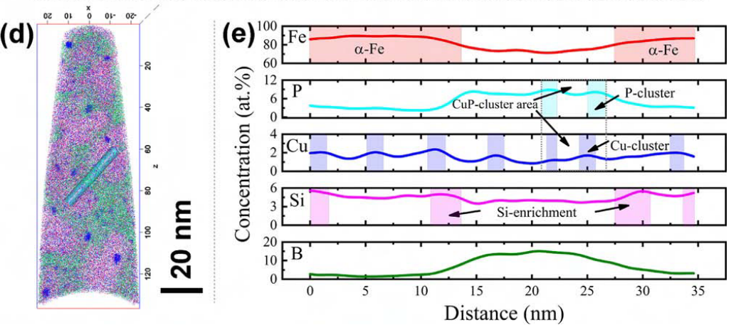
APT element map of Fe 81.3 Si 4 B 9 P 4 Cu 1.7 melt-spun alloy ribbon with (a) element distribution on surface area; (b, d) 2D element distribution map; (c) atomic concen-tration depth profile from the selected region ( Ф 5 nm × 60 nm) in (b); (e) atomic concentration depth profile from the selected region ( Ф 5 nm × 35 nm) in (d).
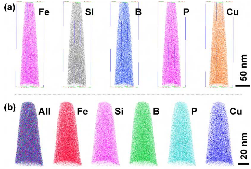
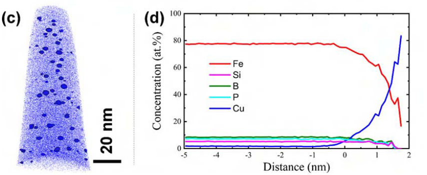
APT element map of Fe 81.3 Si 4 B 8 P 5 Cu 1.7 melt-spun alloy ribbon with element distribution on the (a) inner area and (b) surface area; (c) highlighting Cu with 5 at.% Cu isoconcentration surface; (d) atomic concentration depth profile from a randomly selected region of Cu cluster in (c).
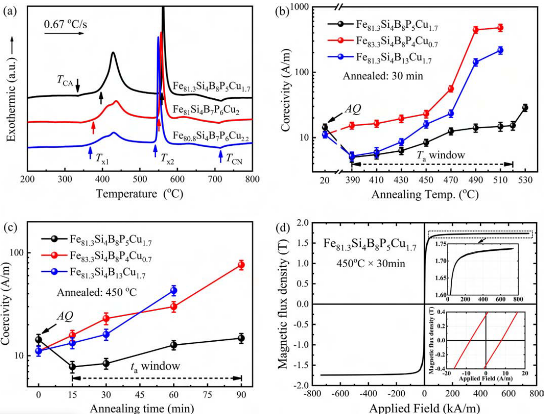
Thermal and soft magnetic properties of FeSiBPCu alloys with (a) DSC curve; the dependence of coercivity on (b) annealing temperature and (c) annealing time;(d) hysteresis loop of Fe 81.3 Si 4 B 8 P 5 Cu 1.7 alloy annealed at 450 °C for 30 min, the inset shows a partial enlargement of that of approaching saturation and hysteresis curve measured by DC B–H loop tracer.
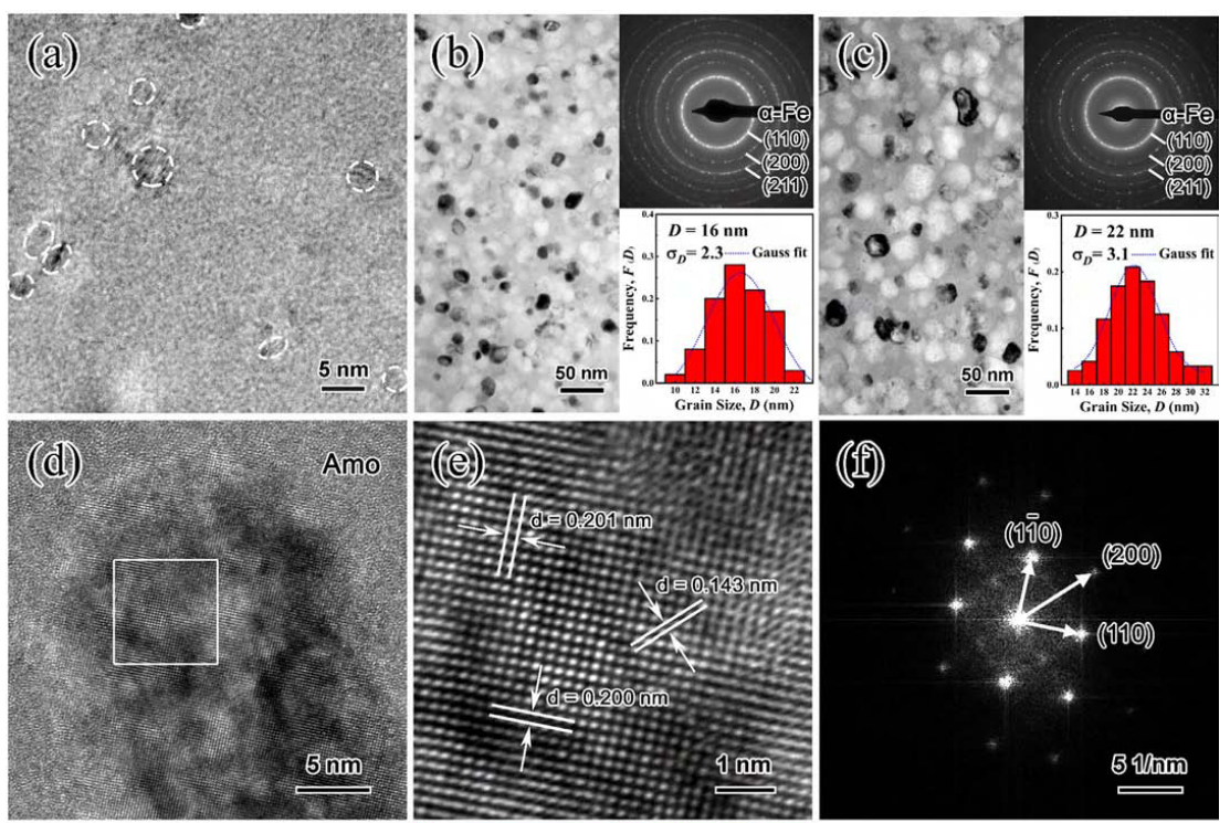
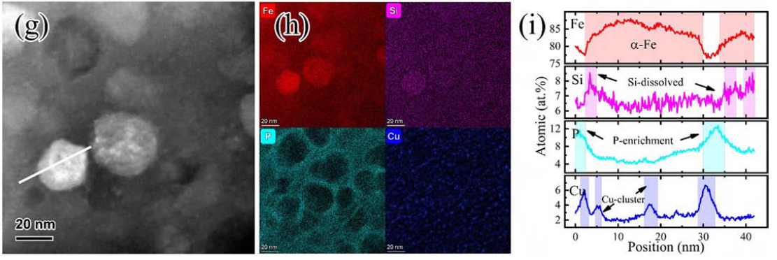
Microstructure of Fe 81.3 Si 4 B 8 P 5 Cu 1.7 alloy with (a) HRTEM image of the melt-spun sample, (b, c) bright field TEM image and corresponding selected area electron diffraction, the grain size distribution of samples annealed at 450 °C for 30 and 60 min, respectively. (d) HRTEM image of the sample annealed at 450 °C for 60 min and corresponding (e) enlarged part of the selected area and (f) FFT image of (d). (g) HAADF-STEM image and corresponding (h) EDS mappings and (i) line scan showing the distribution of Fe, Si, P, and Cu elements for the sample annealed at 450 °C for 60 min.

Schematic diagram of the atomic structure of Fe 81.3 Si 4 B 8 P 5 Cu 1.7 alloy with (a) melt-spun and (b) annealed sample. (c) Schematic diagram of the atomic structure showing: (ca1, ca2) nucleation mechanism and (cb1–cb3) solid solution mechanism.